The ZK Chronicles: Circuits (Part 2)
If you recall, a couple articles back we introduced the circuit satisfiability problem (both versions, CSAT and #SAT), which led us directly into a powerful extension of traditional circuits in the form of arithmetic circuits.
While these problems were interesting in concept, they probably still felt a little awkward. And back then, we claimed that a more intuitive alternative for our purposes was to somehow prove the correctness of a circuit evaluation — you know, proving that evaluating a circuit at a particular set of inputs yields a claimed result.
Our goal for today will be to present a mechanism to do just this.
I must warn you: this will be slightly more involved than previous articles. However, it will lead us to what feels like our very first truly general proving system.
The first of many!
Don’t worry too much though! As always, we’ll take it step by step, piecing apart the important bits.
There’s much to cover, so grab your coffee and sit tight — this will be a long one!
Proving Evaluation
Alright then! Given that we’ve already learned of arithmetic circuits, we can jump right into the problem at hand.
Given some arithmetic circuit , our goal is to prove that for some input , the output of the circuit has some value :
I want us to take a moment to analyze how to approach this.
We don't have any clear hints yet. With #SAT, the hypercube sum made the connection to sum-check obvious, but we don't have the same luxury here. We're gonna need another angle of attack.
Maybe we should recollect our knowledge so far, and that will give us a direction to follow. Let’s see: we know arithmetic circuits are comprised of addition and multiplication gates. And whenever you feed some input to a circuit, it flows forward through the wires and into gates (remember, it’s a DAG), which perform simple operations.
Here’s a quick question: what happens if a gate is miscalculated?
We’re pretty much assuming the “happy path” so far, but what if that wasn’t the case? Any single incorrect calculation of a gate would cause a ripple effect through the circuit, rendering the entire calculation invalid.
Conversely, we can also say that in order for the result of the entire circuit to be correct, each gate must have been correctly computed.
Yes, there’s a tiny chance the result accidentally stays correct due to modulo arithmetic. But with a properly sized field, this probability is negligible, so we can safely ignore it!
This gives us an extremely powerful insight: we can decompose the problem of checking circuit evaluation into checking the correct evaluation of individual gates.
And that’s mainly where the power of circuits as a computation model comes from! Gates are sort of the Lego blocks of verifiable computing: you can check their correctness, and you can chain them together to form richer structures!

Good! This seems like a promising starting point. What we need now is a way to use this newfound knowledge.
Relevant Information
In order to build a proving system, a verifier should be able to probe these gates to check if they are correctly calculated. This is usually done through an encoding strategy: the computation at a gate is somehow expressed in a form the verifier can use on their own.
So how do we do that?
Well, there are at least three things a verifier needs to successfully check whether a gate calculation is valid or not:
- The inputs
- The output
- The type of the gate (either addition or multiplication)
If a verifier can get ahold of these things, they can simply compute the expected output, and compare with the provided result!
That’s the theory, at least — but how would we encode this information?
Encoding
The answer might be unsurprising at this point: polynomials!
It’s always polynomials!
There’s no single way to do this. Different proving systems use different techniques — and that’s part of where the key differences between modern proving systems come from.
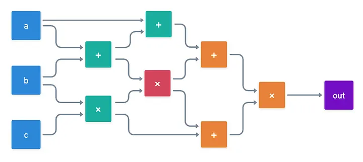
I want us to get our feet wet with an example. Let’s see what we can do with a small circuit:
Here are a few ideas. First, we’d want to encode the wire values. We have a total of wires, so we could create a polynomial such that:
Note that those are evaluations — we’ll say a bit more about how to get the actual polynomial further ahead.
Then, we’d need to encode gate information. To do this, we can use indicator polynomials for each gate: one for addition gates, and one for multiplication gates.
In a similar fashion to Lagrange bases, we can choose a gate , and craft a polynomial that returns only when:
- The values of , , and correspond to the correct wires for the gate, with being the left input, and being the right input, and being the output.
- Gate is an addition gate.
The same can be done with multiplication gates, and a polynomial .
With this, we can represent the statement “gate is correctly evaluated” with this expression here:
The role of and is to sort of deactivate the checks if they do not correspond to the correct gate! Of course, we should ensure that and are not equal to at the same time!
Ok, pause. That was probably a lot of information!
Take a moment to let all this sink in. These kind of encoding strategies will be very important as we move further into the series, so it’s a good idea to get acquainted with them now!
Seriously, take your time. If you skip ahead, I’ll know.

Good? Okay, let's move along!
Gate encoding, check.
Unfortunately... There’s a very blatant problem with this: in order to check the correctness of a circuit evaluation, a verifier would need to check every single gate. For large circuits (where the size is large), this would mean verification time.
And this is pretty bad, because it’s no better than simply running the circuit — and the whole gist of verifiable computing is to allow verifiers to run faster than that!
We’ve stumbled upon a big hurdle on our plans... Can we do any better?
Structured Circuits
Sometimes we can!
The secret lies in realizing that not all circuits are made equal. Indeed, all circuits have a different overarching structure. And in some cases, we can exploit it to achieve a better performance.
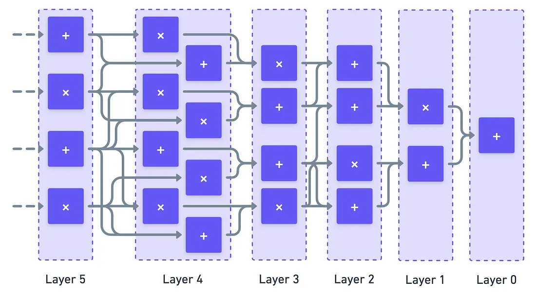
In particular, we’re interested in circuits where we can identify clear layers: groups of gates that are not directly connected to each other (they are independent), and instead depend only on a previous layer.
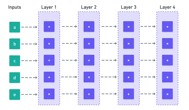
We call the number of layers the depth () of the circuit, and the number of wires in each layer represent the layer’s width (). For circuits with relatively uniform width, the total size of the circuit is roughly .
Now... What would happen if we could show that an entire layer is correctly calculated in a single go?
If we can achieve this, we may be in for sizable time savings — especially for shallow circuits, whose depth is much smaller than their width.
Some protocols indeed take advantage of this structure. Such is the case of our next subject: the GKR protocol.
The GKR Protocol
GKR stands for the initials of the creators of the technique: Goldwasser, Kalai, and Rothblum. Several techniques in cryptography have adopted this way of naming.
Now, this will combine pretty much everything we’ve learned so far: structured circuits, polynomial encoding, multilinear extensions, and sum checks.
From personal experience, my suggestion is not to rush this. Circle back to the previous concepts if needed. This article is going nowhere — that much I can assure you!
Circuit Layout
The GKR protocol assumes a very specific structure for the circuit. Not only is it layered, but every layer has a predetermined number of gates.
Let’s label each layer with an index . Starting from the output layer with an index of , and counting backwards towards the inputs, each layer will have a total of gates.
Note that is a value associated with each layer!
Nothing is unintentional about this choice. But why exactly would we force layers to have such an oddly-specific number of gates?
The reason is one we have already exploited in the past: indexing!
Essentially, we can label each gate (or equivalently, each wire) of any given layer using our trusty boolean hypercube! We encode the values for each gate as evaluations of some function :
Where returns the value on wire in layer ( is a -bit binary string indexing the wire).
And you know what a boolean hypercube means: a sum check is coming!
Connecting the Layers
Of course, the part we’re still missing is that gate operation encoding we talked about before. And to obtain this, we’ll need to do one more thing: specify how gate are connected.
This is referred to as the wiring predicate. It’s the only missing piece in today’s puzzle, and once we have this, we’ll finally be able to connect everything.
Quite literally!
For this, let’s define the polynomials and , which describe this wiring predicate:
These, as previously stated, will take three gate labels , , and — the first two from the input layer, and the last one from the output layer — , and return only when:
- The gates in the combination are truly connected in the circuit, meaning that gate has inputs and .
- The rightmost gate () is of the correct type (addition or multiplication).
Similarly, for multiplication gates.
While encodes the values of wires in layer , , describe which gates connect to which, and their types. Together, they constitute a complete description of the circuit, or a full encoding!
All that remains, as hinted earlier, is to somehow transform this into a sum check.
Building the Sum Check
If you recall, the sum-check protocol had a very nice recursive structure: the original problem was reduced into a smaller version of the same problem, ultimately having something that’s almost trivial to check.
So, how about we try something along those lines?
The idea is simple: start at the output layer, with some claimed output values. There, we’ll try to transform the claim about the outputs, into a claim about the values of the second-to-last layer. Rinse and repeat, and after steps, we get to a claim about the inputs, which should be known by the verifier!
Simple, right?

Stay strong folks!
To perform this reduction step, we’ll need to check something about each layer. And this is where our encoding becomes relevant, all thanks to this little trick here:
Before your head explodes, let’s just try to explain what the expression is doing:
- We’re summing over all the possible gate indexes at layer , which are the possible inputs at layer (the output layer in this step)
- Then, we’re asking: is this an addition gate or a multiplication gate? Remember, and return either or , and they will only activate when a gate with inputs and , and output exists on the layer, **and **when the gate is of the specified type.
- Lastly, and are multiplied by the desired operations.
The key point here is that despite summing over a boolean hypercube, only one of the possible combinations will activate or — so the entire sum reduces to only one term.
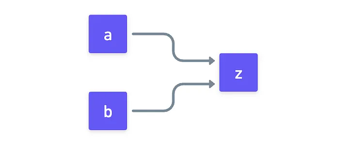
For example: if wire at layer gets inputs from wires and at layer via an addition gate, then we have that:
- The entire sum reduces to just !
Now, the similarities with the sum check are much more evident!
That crazy polynomial inside the sum? Let’s just call it :
And with it, we could fix to a particular value, and apply the sum-check to verify:
Note that we’re fixing so that the wiring predicate makes sense!
As you can see, at each layer, we need values from the next layer to build this polynomial we’re using. Unless the verifier is looking at the input layer, they would not know these values! Instead, the prover will provide them — so this sum check reduces the problem to a claim about the next layer!
Thus, we only need to apply this times (the depth of the circuit), and we’d be pretty much done.
The Remaining Challenges
Okay, great! This is shaping up quite nicely. But to move forward, we’ll need to address two remaining problems, that become clear once we take a closer look at the sum-check we need to perform in any single layer.
So, let’s briefly recap how the sum-check protocol proceeds.
- First, the prover sends a claimed result and a univariate polynomial to the verifier, crafted from the original .
- The verifier performs a simple check, and then selects a random challenge at which they evaluate . They also send this value to the prover.
- The prover then proceeds to prove that is the new claimed result — and they do so by circling back to (1.)!
The process is repeated until all variables of the original are used up, and the verifier closes the process by performing a single oracle query. Of course, in our case, is the for each layer.
For the full explanation, you can go back to this article!
Now, this mechanism has two problems:
- We need to be able to evaluate in a point randomly selected from a large finite field... But by definition, this polynomial is defined over a boolean hypercube!
- The final oracle query can actually be computed by the verifier, so long as they know two special values: the evaluation of in the previous layer at the randomly selected points. But these values are not known by the verifier!
If we manage to solve these problems, then we’d have a fully functional proving system. Let’s tackle them one at a time.
Going Multilinear

So, we need to apply the sum-check protocol on that long expression encoding the wiring predicate:
During the sum-check, we need to be able to select random values selected from a finite field for each component of the inputs. That means we’ll need to extend the domain of those polynomials!
While there are multiple ways to do this, there’s an elegantly simple and performant way to do it: multilinear extensions (MLEs). If we take MLEs of every involved polynomial, we get an expression that’s suitable for our needs:
Oh, by the way, we denote multilinear extension with the tilde () symbol, so is the multilinear extension of W (defined over a more constrained domain, like a boolean hypercube).
Regarding the above equality, feel free to check if it holds if you’d like!
And with this, we're able to perform a sum-check on each layer!
Reducing Evaluations
Lastly, remember that the oracle query at the very end of each sum-check (for each layer) requires two evaluations of the previous layer, on some randomly-selected input:
Now, if we had to perform two checks every time, the number of times we’d need to run the full sum-check would grow exponentially, making our strategy unusable. Therefore, the final touch in our mechanism is to try and combine those two checks into a single one!
This will be a useful tool in other contexts, so I’ll link back to this section in the future. Don’t worry!
We can use a very clever trick for this. Define:
This is simply a line. And we already know a line is defined by two points. We can set those to be , and .
Now this line encodes both values.
With this, we’ll define a little subprotocol. Here’s how it goes:
- The prover sends a univariate polynomial of degree at most , claimed to equal:
- The verifier then checks that , and . This validates that at the very least, this claimed polynomial encodes the required values.
- Finally, the verifier chooses some random point , and with this they calculate:
So, what’s happening here? The prover is essentially providing a way for the verifier to “safely” evaluate for the next layer’s sum-check:
Note that this check does not correspond to selecting a random layer on the next layer. Instead, we use some random value which most probably won’t lie at a valid gate index, but rather on some other point!
The key idea is that the prover does not know in advance. Because of this, if is actually incorrect (let’s call it ), we know thanks to the Schwartz-Zippel lemma that it’s very likely that:
This will make life very hard for the prover, who has to continue with the next round of sum-check with a wrong claimed sum, for which they could not use the actual wire polynomials.
With these two considerations in mind, the protocol is completely defined!
The flow goes:
- The prover encodes circuit layers as polynomials, and calculates their multilinear extensions.
- Starting on the last layer, prover and verifier engage in a round of sum-check, using the output value as the initial claim.
- The prover reduces the two required evaluations to a single one via , which they send to the verifier. The verifier then calculates the claim for the next round of sum-check.
- Rinse and repeat until the input layer is reached, at which point the verifier can close the verifications on their own (no oracle access is needed!).
Analysis
As always though, we need to assess a few key aspects about the protocol to determine whether it makes sense or not: namely completeness, soundness, and cost analysis.
I know you guys might be tired at this point. This is already a knowledge bomb as it stands.
tl;dr: GKR is sound with negligible error, verifier runs in roughly , but prover is expensive at . If you want the details, read on. Otherwise, skip to the summary!
Soundness
Completeness does not need much explanation: as long as the prover is honest, all the expressions we presented should work. Soundness however does take some more work to show.
Pretty much as always!
At each layer , the prover could lie about:
- The polynomials sent during the sum-check. We know these to have degree , so using the Schwartz-Zippel lemma, there’s a that the prover gets lucky over the random choice of the verifier — essentially the same logic we used here.
- The line reduction . Because is at most a -degree polynomial, we can once again use the Schwartz-Zippel lemma, and calculate the probability of a random coincidence over the choice of to be at most .
Once caught in a lie on a given layer, the prover must continue to the next layer with an incorrect claim. They’d need to get lucky at every subsequent layer to avoid detection. Which means that for the full circuit, the total soundness error is the sum of the errors at each layer.
This results in . What can we make out of this value? Essentially, that we can make this error arbitrarily small with an adequate selection of ! In other words, the bigger the size of , the smaller the soundness error will be.
So the GKR protocol is sound!
Costs
The other important aspect to discuss are the computational costs for the full protocol. This will determine if the protocol has any chance of being useful at all.
To explain the costs however, we’d need a couple lemmas and ideas we haven’t yet presented. I don’t think it wise to keep packing content onto this single article, and we might get a chance to talk about this in the future. So instead, again, I’ll summarize the costs for you guys:
- The prover runs in time.
- The verifier, simplifying a bit, runs in , where is the cost to evaluate the input layer’s MLE.
- Total communication costs are field elements.
Of course, it’s important to understand where these numbers come from — but I promise we’ll continue improving our estimation logic as we go further into the series!
What’s most important now is to assess the verification time gains when applying the GKR protocol. Note that the prover is really slow: cubic time means that their runtime will grow quite large even for not-so-large circuits.
The verifier, however, benefits dramatically when the circuits are shallow, meaning their depth is small.
Just to throw some numbers in: for a circuit of size (about 1 million gates) and depth , the prover will run in roughly operations (which is extremely expensive), but the verifier runtime will only be roughly , which is much smaller!
And the number of field elements that are communicated is even smaller: just !
While this sounds good in principle, truth is that the GKR’s prover cost are still prohibitively high for large circuits. This becomes a bottleneck for its applicability, especially due to its interactive nature.
For this reason, practical implementations focus on certain optimizations, or preprocessing steps that bring down prover costs to a more manageable level — but that, my friends, will be a story for another time.
Summary
Oh my God. That was a long one.
But we did it!

We’ve just seen our first truly general circuit verification protocol. And despite its runtime limitations, GKR reveals something super important: that fast verification of arbitrary computations is possible.
This is a crucial stepping stone in our journey towards more practical protocols. Our goal moving forward will be to find better ways to encode and verify computations, but at least we now know it can be done.
I think this is a powerful moment in our journey. I invite you to take a moment to appreciate how much we’ve done with just a couple tools. Just imagine what crazy things we’ll get into later!
Speaking of which, we have solely focused on circuits as our general computation models for now. I don’t know about you, but for me, writing a circuit does not feel like the most natural thing to do when writing a program. We normally think of computation in other terms.
So, does that mean that our efforts are fundamentally flawed? This is a question that we’ll try to answer in our next encounter!
See you soon!
Did you find this content useful?
Support Frank Mangone by sending a coffee. All proceeds go directly to the author.